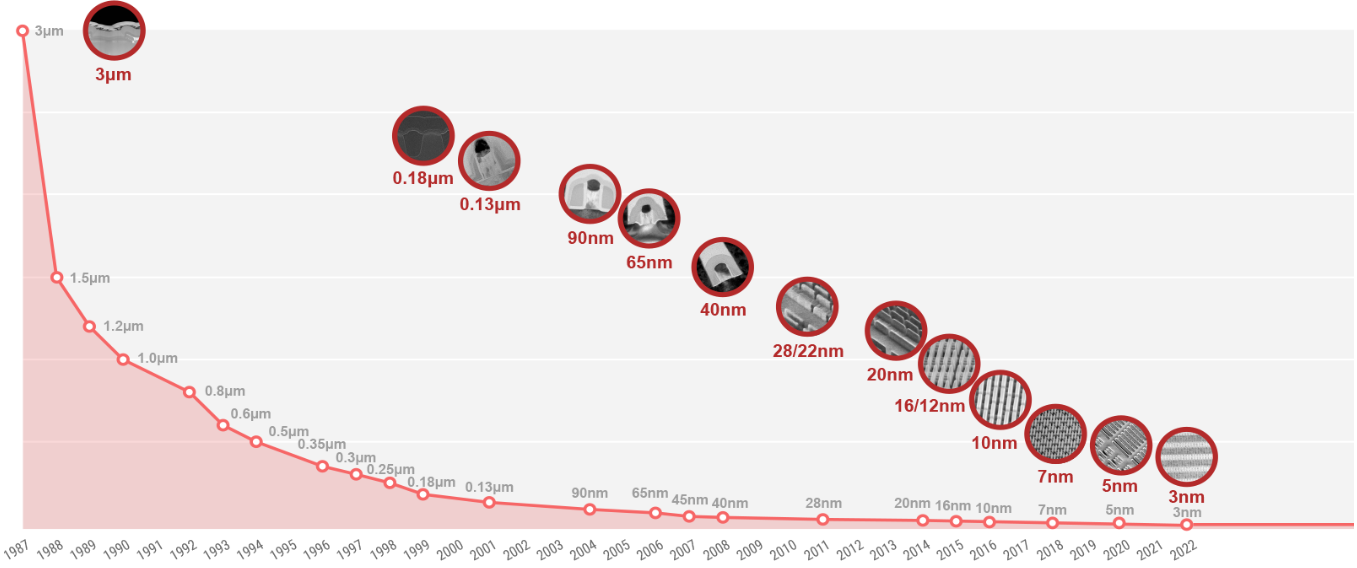
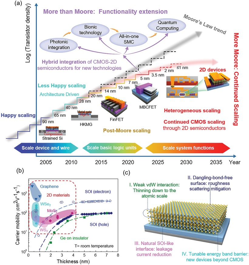
In the dynamic world of electronics, the term “technology node” has become a centerpiece, referring to the specific set of semiconductor fabrication processes that define the dimensions and capabilities of silicon chips. Historically, the relentless pace of advancement in this domain has been astutely summarized by Moore’s Law. Coined by Gordon Moore, co-founder of Intel, in 1965, Moore’s Law observed that the number of transistors on a microchip double approximately every two years, propelling an exponential surge in computing power while the costs are halved. As we journey through semiconductor evolution, from its nascent stages to the cutting-edge nodes of today, we must appreciate the monumental technological feats achieved and anticipate the groundbreaking innovations on the horizon.
From Humble Beginnings: Understanding Technology Nodes, the chronicle of technology nodes began with the inception of the semiconductor industry in the 1960s. The “node” refers to a specific generation of semiconductor manufacturing processes, traditionally indicating the length of the smallest feature that can be manufactured on a chip. This feature was often the gate length of a transistor, starting at the micrometer scale (1-micron, 800nm, 600nm…) and advancing to the current era where dimensions are expressed in nanometers (nm) – such as 7nm, 5nm, and even 3nm nodes.

Moore’s Law
The Guiding Beacon For decades, Moore’s Law has not only been an observation but also a self-fulfilling prophecy guiding the semiconductor industry. This biennial doubling of transistor density has driven continuous enhancements in performance, energy efficiency, and cost-effectiveness of electronic devices, from the simplest calculators to the most sophisticated supercomputers. It’s a testament to human ingenuity, showcasing our relentless pursuit of technological progress. However, as technology nodes continue to shrink, we inch closer to the physical limitations of materials and the laws of physics. The challenges include excessive heat generation, increased power leakage, and quantum tunneling, where electrons travel unpredictably as components reach atomic scales.
The Latest Advancements
Defying Boundaries Despite these challenges, the industry’s brilliant minds continue to push the envelope. Several groundbreaking techniques have been developed to maintain the momentum of Moore’s Law:
- EUV Lithography: Extreme Ultraviolet (EUV) lithography is a revolutionary approach that uses extremely short wavelengths of light to etch finer patterns onto silicon wafers, enabling the continuation of node shrinkage, pivotal for the 7nm node and beyond.
- 3D Stacking: As lateral scaling becomes more challenging; manufacturers are looking vertically. Through techniques like 3D stacking, multiple layers of active electronic components are stacked on top of one another, improving performance and functionality per unit area.
- New Materials and Transistor Designs: Incorporating new materials like graphene and carbon nanotubes, and innovative transistor designs such as Gate-All-Around FETs (GAAFETs) and Nanosheet transistors, engineers are finding ways to reduce leakage and power consumption while boosting performance.
- 2nm and Beyond: Leading companies like TSMC, Intel, and Samsung are not just stopping at the 5nm or 3nm node; they are actively developing the 2nm technology node and researching even more advanced nodes. These future nodes promise further improvements in performance, power, and area (PPA), albeit with increasing complexity and manufacturing challenges.
Conclusion
The Future Beyond Moore’s Law While the journey through semiconductor technology nodes guided by Moore’s Law has been remarkable, the industry recognizes that this pace of advancement cannot continue indefinitely with the current methodologies. The focus is gradually shifting from mere scaling to heterogeneous integration – combining different types of devices and technologies, optimizing systems rather than just transistors.

Additionally, the rise of quantum computing, neuromorphic computing, and the use of AI in chip design signifies that the future might not be a straightforward path down the nanometer scale. It will be an interdisciplinary convergence, an amalgamation of novel computing paradigms, and a holistic advancement in information technology systems. As we stand on the precipice of this new era, one thing remains certain: the spirit of innovation that has propelled us from the first technology node will continue to drive humanity’s technological prowess into uncharted territories. The semiconductor industry’s journey is far from over; it’s merely embracing new directions.

 Semiconductor FAB Solutions
 OEM Solutions