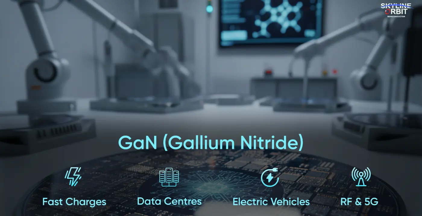
GaN – Next Generation III-V Material for Semiconductor Industry
Silicon has been a common yet unique material driving the electronics industry for the last 60 years. Most IC chips in mobiles and high-speed laptop processors use silicon material. The major factor behind using silicon to make transistors on an IC is its unique semiconducting properties and abundance on Earth. Silicon is the second most abundant material available on Earth and can be used for various applications[1].
Moore’s law states that the number of transistors per chip doubles approximately every two years [2]. Over the last 20–25 years, scientists and engineers around the world have made significant progress in silicon-based devices and reached very close to the theoretical limit of Moore’s law. This means that to increase the number of transistors or the performance of devices, researchers must find a new material that can be used to make semiconductor components for ICs with improved device performance.
The answer to the question “Why not silicon anymore?” may be that we need a material that can replace Si with better electronic properties and enhanced device performance.
GaN is a very promising material that can replace silicon in next-generation electronic devices with better performance. GaN is the leading candidate for taking electronic performance to the next level. In this article, the major advantages of GaN over silicon, various applications, and the manufacturing process for GaN devices are covered.
Explore how Orbit & Skyline supports next-gen semiconductor innovation through Semiconductor FAB Solutions including equipment and process engineering.
What is GaN (Gallium Nitride)?
GaN is one of the compound semiconducting materials from the III-V group of materials. Ga is a group III element, and N is a group V element from the periodic table. Combining these group materials together with a suitable method results in a compound material commonly known as a III-V or compound semiconductor. GaN has unique electrical, mechanical, and thermal properties, which make it superior to commonly used materials like Si for different electronic applications.
Gallium nitride (GaN) is a wide bandgap semiconductor material with a hard, hexagonal crystal structure. Bandgap is the energy needed to free an electron from its orbit around the nucleus, allowing it to become free and take part in electron conduction.
Key Advantages of Gallium Nitride (GaN) Over Silicon (Si)
Tunable Bandgap, Higher Speed, Higher Thermal Stability, High Breakdown Voltage
One of the advantages of gallium nitride over silicon is its large, tunable bandgap. Gallium nitride has a bandgap of 3.2 electron volts (eV), compared to silicon’s bandgap value of 1.1 eV.
The bandgap defines the electric field that a semiconducting material can withstand. A wide bandgap in GaN enables the development of semiconductors with very short or narrow depletion regions, leading to device structures with very high carrier density. With this property, smaller transistors with shorter current paths, very low resistance, and capacitance are achieved, enabling speeds much faster than silicon-based devices.
This higher bandgap value allows GaN to have very high breakdown voltages and good thermal stability at elevated temperatures. GaN-based electronic devices can withstand higher temperatures, enabling their use in very harsh environments. GaN-based materials have applications with voltages between 100 V and 600 V, allowing the use of smaller, more efficient chips that reduce costs and carbon emissions.
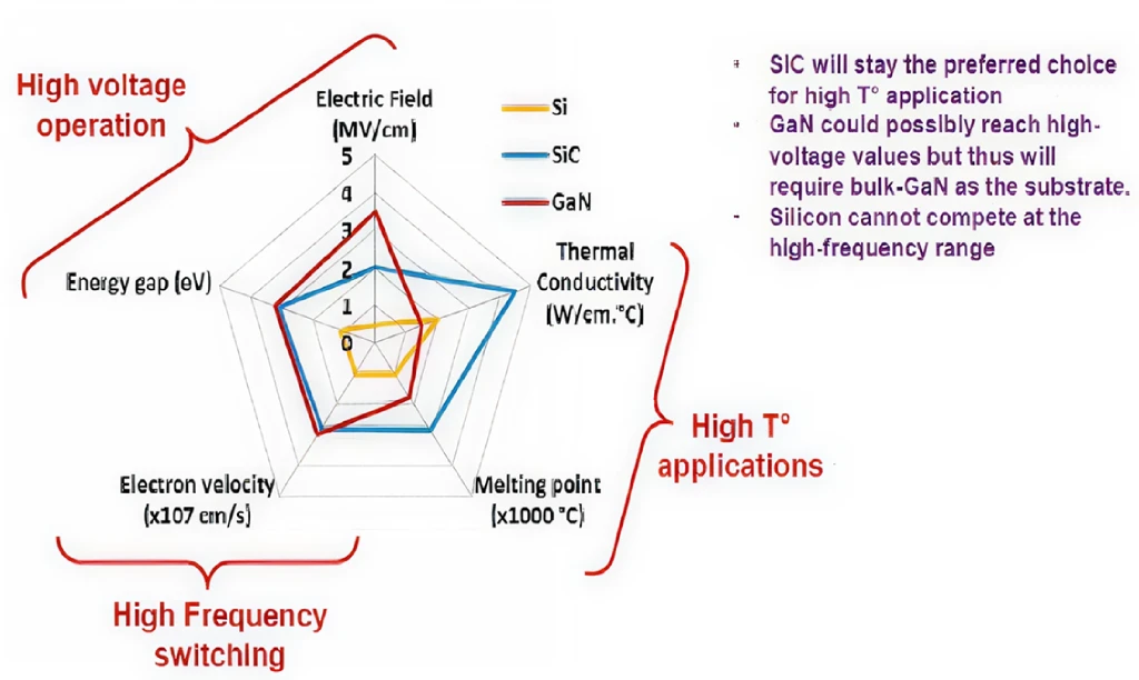
GaN’s breakdown field is 3.3 MV/cm, much higher than silicon’s 0.3 MV/cm. This high breakdown voltage allows GaN materials to withstand very high voltages without affecting device performance. Therefore, GaN devices can be used in applications that require high voltages for their operation.
Another advantage of GaN over silicon is its high electron mobility. GaN materials have the ability to conduct electrons more than 1000 times more efficiently than silicon while being able to be manufactured at a lower cost[3]. Higher mobility allows charge carriers or electrons in gallium nitride crystals to move much faster than in silicon. This makes GaN-based transistor action much faster than Si-based transistors. As a result, mobile phones, computer processors, and chargers will be faster, improving overall device performance.
Orbit & Skyline’s Process Engineering Services help optimize material performance parameters like mobility, breakdown voltage, and thermal stability in compound semiconductor manufacturing.
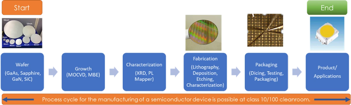
Manufacturing Process for GaN-based Electronic Devices
Manufacturing GaN-based devices requires high capital investment together with sophisticated tools, quite similar to those used in Si-based manufacturing processes. GaN-based electronic devices can be made using GaN, Sapphire, SiC, or Si wafers. Currently, researchers are working on devices with GaN material on top of large-area Si wafers. These different wafer types have certain advantages and disadvantages, which are not covered in this article. Most GaN-based products are made using either Sapphire or SiC wafers, as the production cost of pure GaN wafers is very high. This high cost is because GaN does not occur naturally by itself.
The manufacturing process is not as simple as the well-established Si-based process, but researchers around the world are working to improve it.
Uses and Applications of GaN in Semiconductor and Power Electronics
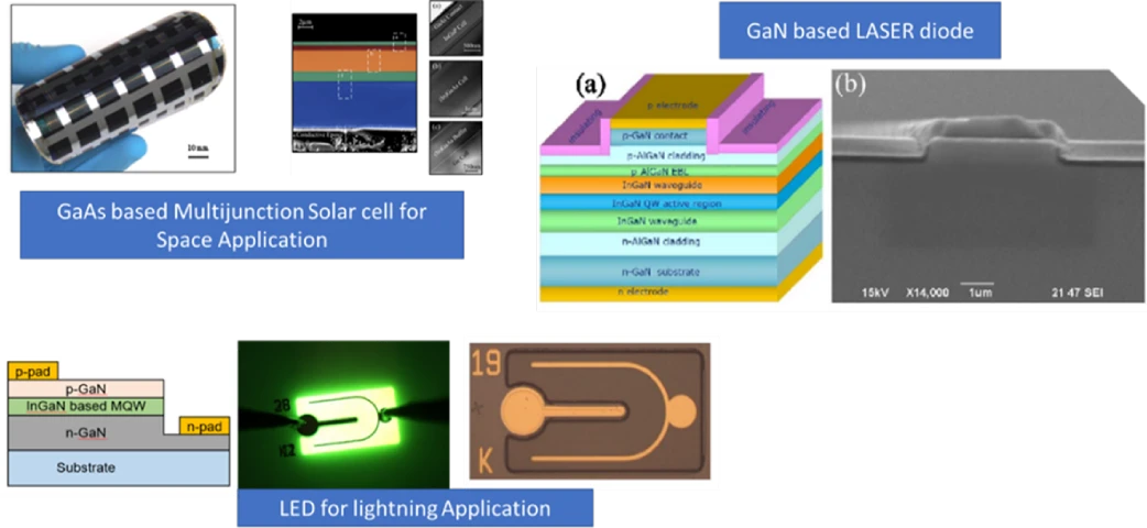
Gallium nitride has widespread applications in electronics, display, switching, and power systems. Various applications include LEDs, LASERs, Diodes, HEMTs, and RF devices.
GaN-based blue light-emitting diodes are commonly used for lighting applications. The 2014 Nobel Prize in Physics was awarded to Shuji Nakamura, Isamu Akasaki, and Hiroshi Amano “for the invention of efficient blue light-emitting diodes, which have enabled bright and energy-saving white light sources”[4]. These LED chips used GaN materials as the light-emitting layers.

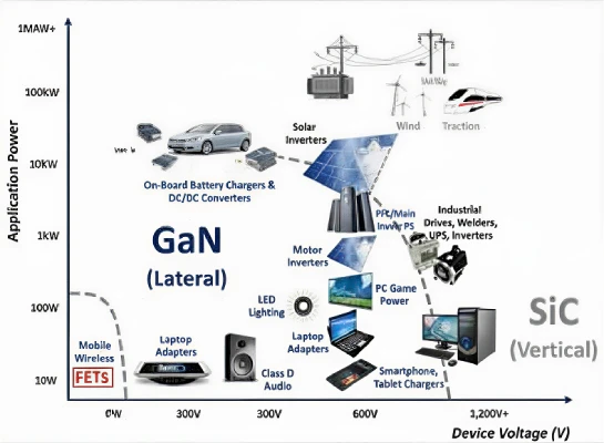
Another area of application for GaN materials is radio frequency (RF) devices. GSM and Wi-Fi signals in mobiles and computers are transmitted and received using GaN-based RF devices.
GaN-based chips are also used in mobile chargers and laptop adapters, providing faster charging with smaller size and lighter weight. Silicon-based chargers dominate the current mobile industry, but GaN-based chargers offer faster charging speeds with reduced size and weight. GaN fast chargers have been released by Tier-1 OEMs such as Dell, Lenovo, Samsung, Xiaomi, LG, and OPPO, as well as by aftermarket companies including Belkin, Anker, AUKEY, Hyper, and Baseus.

Conclusion
GaN is shaping the future of electronics with its efficiency, speed and ability to perform where silicon reaches its limits. From power devices to communication systems, it is enabling more compact, reliable and energy-efficient technologies across industries.
With 15+ years of expertise and a global team of 500+ engineers, Orbit & Skyline is a trusted partner in the semiconductor industry. If you are looking for a semiconductor services and solution partner, reach out to us at hello@orbitskyline.com.
References
- [1] Wikipedia. [Online]. Available: https://en.wikipedia.org/wiki/Abundance_of_the_chemical_elements
- [2] Wikipedia. [Online]. Available:https://en.wikipedia.org/wiki/Moore%27s_law
- [3] [Online]. Available:https://epc-co.com/epc/GalliumNitride/WhatisGaN.aspx
- [4] Wikipedia. [Online]. Available: https://en.wikipedia.org/wiki/Shuji_Nakamura
- [5] [Online]. Available: https://www.navitassemi.com/gallium-nitride-the-next-generation-of-power/
- [6] [Online]. Available: https://www.navitassemi.com/gallium-nitride-the-next-generation-of-power/

 Semiconductor FAB Solutions
 OEM Solutions