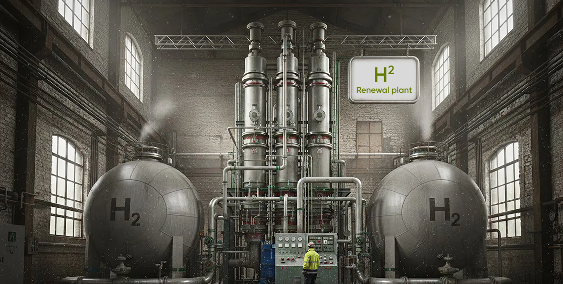
The Future of Clean Manufacturing: Where Hydrogen Meets Semiconductor Technology
Hydrogen has long been an essential element in semiconductor manufacturing, and its role is becoming even more important as clean technology industries evolve. Modern chip fabrication depends on hydrogen to maintain ultrapure processing environments and to support critical steps such as wafer cleaning, annealing, and epitaxial growth. These processes demand extremely stable and contaminant free conditions, which hydrogen helps achieve.
At the same time, advances in semiconductor materials are enabling the next generation of green hydrogen technologies. High efficiency photocatalysts, photoelectrochemical cells, and solar driven electrolysis systems all rely on semiconductor structures to convert light into chemical energy more effectively. As these semiconductor-based systems improve, they make large-scale green hydrogen production more practical and cost-effective.
Together, these trends show how hydrogen and semiconductor manufacturing are becoming part of a mutually reinforcing cleantech cycle: hydrogen supports the production of advanced semiconductor devices, while semiconductor innovations accelerate the development of cleaner hydrogen generation methods and strengthen the broader hydrogen economy.
Hydrogen in Semiconductor Manufacturing
Hydrogen is not just a process gas. It plays a key role in maintaining cleanliness, precision, and reliability during semiconductor wafer manufacturing. It is widely used in thermal processing, thinfilm deposition, and lithography, and supports multiple critical steps throughout wafer fabrication. Without dependable hydrogen handling, achieving high yields at advanced nodes becomes much harder.
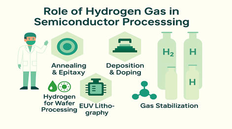
Hydrogen in Annealing and Epitaxial Growth
High-temperature annealing and epitaxy use hydrogen to keep the process stable and control defects. At temperatures above 1,000 °C, hydrogen helps to maintain uniform heat transfer and removes native oxides by acting as a reducing agent, which improves interface quality. It also passivates surfaces and stabilizes precursors, reducing the chance of defects in epitaxial layers.
Studies show that hydrogen assisted epitaxial growth can reduce dislocation density by 30–40%, improving electron transport and reducing wafer loss.[1]
Hydrogen in CVD and Doping
For CVD and PECVD, hydrogen passivates dangling bonds, suppresses minority carrier recombination at stacking faults, reduces interface trap density, and limits oxygen contamination, resulting in higher quality films and improved electrical characteristics. H2N2 forming gas anneals, a longstanding method for CMOS reliability, remain essential at advanced nodes.[2]
Hydrogen in EUV Lithography cleaning process
In EUV lithography, hydrogen maintains optical performance. In laser-produced plasma (LPP) sources, tin debris accumulates in the plasma chamber and deposits on collector mirrors. In semiconductor manufacturing, hydrogen reacts with tin to form volatile SnH4, which is removed through vacuum. This hydrogen based cleaning process preserves mirror reflectivity and extends component lifetime, which is essential for throughput at sub-5nm patterning.[3]
Hydrogen in Gas Stabilisation
Hydrogen is commonly used to improve the stability of reactive gases like diborane (B2H6) and digermane (Ge2H6) in semiconductor processes. By slowing their decomposition, it enables consistent and controlled doping. As a result, hydrogen-based semiconductor fabrication maintains parts per trillion (ppt) impurity levels and reduces oxygen and moisture ingress.[1]
Hydrogen’s Growing Role in Next-Generation Semiconductor Manufacturing
From annealing and epitaxy to deposition, doping, lithography, and precursor preparation, hydrogen serves multiple roles in semiconductor processing. It acts as a reducing agent, passivates surfaces, supports heat transfer, and helps stabilize reactive gases, which enables clean and defect-controlled fabrication.
Hydrogen will become even more important, as semiconductor manufacturing moves toward wide-bandgap materials like SiC and GaN. These materials require higher processing temperatures, tighter impurity control, and precise doping. Since they are key to next-generation power electronics and electric vehicles, hydrogen plays a significant role in maintaining device performance and long-term reliability.
Semiconductor Materials Shaping the Future of Hydrogen Production
As new semiconductor materials emerge, they are directly influencing and improving modern hydrogen generation methods. Their optical, electronic, and catalytic properties make them effective for carbon-free hydrogen production using sunlight or electricity in green hydrogen technologies.
Semiconductor Materials Enabling Green Hydrogen for Cleanroom Manufacturing
Photoelectrochemical (PEC) Water Splitting:
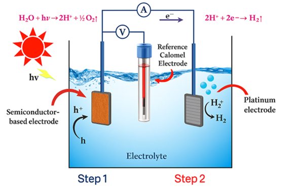
Principle: In PEC water splitting, semiconductor photoelectrodes absorb sunlight and convert that energy directly into the chemical reactions needed to split water into hydrogen and oxygen. This allows solar energy to be directly converted into fuel.
Recent Progress and Advances: High-efficiency photoelectrodes (TiO2, BiVO4, GaN nanowires, and perovskite–silicon tandem structures) have now achieved solar to hydrogen (STH) efficiencies in the 15–20% range. With protective ALD surface coatings, these systems can operate stably for more than 1,000 hours.[4]
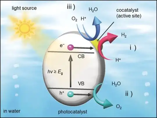
Photocatalytic Water Splitting
Principle: Photocatalytic water splitting uses semiconductor powders/nanostructures as light-activated catalysts to convert sunlight direct into chemical energy. These materials can split water into hydrogen without an applied electrical potential, enabling low cost and distributed production.
Recent Progress and Advances: Engineered nanostructured photocatalysts (gC₃N₄, GaN, ZnIn2S4) with catalysts and cocatalysts now reach quantum efficiencies above 10%, enabling large scale green hydrogen production.[5]
PV-Electrolyser Hybrid Systems for fabs
Principle: PV–electrolyser systems combine high-efficiency photovoltaic cells with electrolysers to convert solar-generated electricity into hydrogen gas. This approach uses advances in semiconductor technology to produce clean, scalable hydrogen and is currently among the most commercially developed routes in the field.
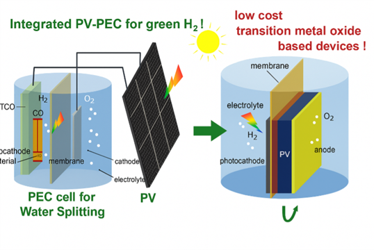
Recent Progress and Advances: PV–EL systems are among the most effective hydrogen generation pathways, supported by advances in semiconductor technology. Perovskite–silicon tandem solar cells now reach solar to hydrogen conversion efficiencies above 20%, producing sufficient electricity to operate PEM or alkaline electrolyzers.
Because PV–EL systems are modular, durable, and increasingly cost efficient, they are well suited for onsite green hydrogen production in semiconductor fabs, data centres, and integrated clean energy facilities.[6]
This approach creates a direct link between today’s energy systems and future hydrogen-powered semiconductor fabs. These systems use precision doping, heterostructure design, and interface passivation from semiconductor device engineering, effectively bridging the two technologies.
Circular Hydrogen-Semiconductor Clean-Tech Ecosystem for Net-Zero Manufacturing
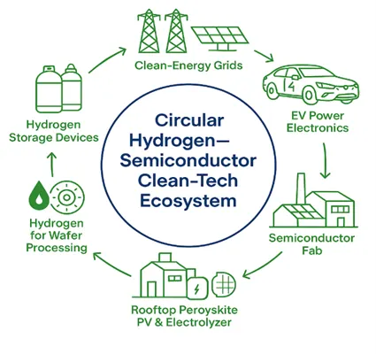
Hydrogen technologies and semiconductor fabrication are closely linked within modern low-carbon manufacturing. In advanced fabs, hydrogen enables the ultraclean process environment required for precise silicon chip production. Meanwhile, semiconductor-based solar cells are generating renewable hydrogen by converting sunlight directly into energy.
Their combined development forms a sustainable loop in which improved materials, integrated systems, and circular processes support low-carbon manufacturing and the transition toward producing chips with near-zero emissions.[3]
Current Synergy and Pilot Deployments
Pilot installation reporting a 30% reduction in emissions have used solar-powered electrolyzer units installed next to semiconductor fabs.[3] These projects demonstrate how onsite hydrogen generation can be connected with semiconductor manufacturing to lower environmental impact while maintaining the purity standards required for fab operations.
Infrastructure and Circular Vision
The vision of a circular clean technology ecosystem for semiconductor manufacturing enabled by onsite green hydrogen production is steadily moving closer to implementation. Advances like rooftop perovskite PV systems, local hydrogen storage, continuous purity monitoring, and recycling loops indicates a pathway toward nearly carbon-neutral fabrication. This framework can also be applied to electric vehicles, power electronics, and wider clean energy industries, where hydrogen and semiconductor innovations support longterm decarbonization.
Future Innovations and Policy Drivers
Next-generation facilities are expected to use AI-driven hydrogen purity control systems that handle purification, real-time monitoring, and stable purity levels that meet regulatory standards. These improvements will cut waste and improve overall process efficiency. Semiconductor recycling programs will also help to close the loop for rare materials like gallium and indium, reducing dependence on primary extraction. Global policies, including carbon-neutral targets and incentives for hydrogen infrastructure will push wider adoption and encourage international collaboration. Together, these developments will position circular clean technology manufacturing as a key element of sustainable industrial growth.
Emerging Trends and Industry Challenges
1) Decentralised, On-Site Hydrogen Production for Semiconductor Fabs
Semiconductor fabs are installing modular, renewable-powered electrolyzers to reduce dependence on external hydrogen suppliers. [3]
Challenge: Maintaining impurity concentrations under 1 ppb in advanced semiconductor fabs remains a significant challenge.[2]
Solution: Inline sensing and AI-based hydrogen quality control systems are emerging to enable continuous monitoring and ensure compliance with regulatory purity requirements.[3]
2) Electrolysis Powered by Renewable Energy
Integration of perovskite-silicon PV arrays with PEM electrolysers enables on-site production of green hydrogen.[6]
Challenge: High costs and variable solar input affect system reliability.[4]
Solution: Hybrid PV-battery systems and advanced electrolysers increase uptime and improve cost efficiency.[6]
3) Advanced Hydrogen Gas Purification and Management in Semiconductor FABs [3]
In advanced fabs, automated hydrogen delivery systems with predictive analytics are being deployed.
Challenge: Scaling purification to achieve ppt-level impurity control without high energy consumption.
Solution: Membrane-based purification and catalytic getters lower energy use while maintaining purity.
Hydrogen vs Conventional Gas Processing in Semiconductor Manufacturing
| Parameter | Hydrogen Gas Processing | Conventional Gas Processing (N2, Ar, Forming Gas Alternatives) |
|---|---|---|
| Role in Annealing | Acts as a reducing agent, removes native oxides, and supports defect passivation | Primarily inert atmosphere control, limited oxide reduction capability |
| Surface Passivation | Dangling bond passivation reduces interface trap density | Limited passivation; often requires additional chemical treatment |
| Thermal Conductivity | High thermal conductivity enables uniform heating above 1000°C | Lower thermal conductivity; less efficient heat transfer |
| EUV Lithography Cleaning | Reacts with Sn debris to form volatile SnH4, maintaining collector mirror performance | Cannot chemically remove tin contamination |
| Doping Stabilization | Stabilizes reactive precursors such as B2H6 and Ge2H6 for controlled doping | Limited chemical stabilisation; higher decomposition risk |
| Impurity Control | Supports ppt level impurity control in advanced fabs | Typically supports ppb-level environments |
| Compatibility with Wide Bandgap Materials (SiC, GaN) | Highly suitable due to high-temperature and impurity sensitivity requirements | Less effective for ultra-high temperature processing |
| Sustainability Impact | Can be sourced from renewable hydrogen pathways | Often sourced from fossil-derived industrial gases |
| Energy Efficiency | Supports cleaner reactions and reduces rework | Higher defect rates may increase energy and material waste |
| Future Scalability | Supports sub 5nm and advanced node processing | Limited scalability for next-generation nodes |
Growing towards a Net-Zero Future for Clean-Tech Manufacturing with Hydrogen and Semiconductors
Hydrogen energy and semiconductor manufacturing are beginning to converge in such ways that are shaping a new phase of industrial development. Inside fabrication facilities, hydrogen helps maintain the ultraclean process conditions required for precise chip production. At the same time, improvements in semiconductor technology are enabling scalable, high yield green hydrogen generation.
Together, these trends form a reinforcing cycle. Hydrogen supports cleaner, renewable powered manufacturing, while advances in semiconductor technologies continue to raise the efficiency and output of hydrogen production systems.
This combination enables cleaner fab operations and long term industrial sustainability.
Hydrogen and Semiconductor Technologies Converging for Net-Zero Manufacturing
Integrating hydrogen technologies with semiconductor manufacturing reflects a transition toward improved energy security and reduced carbon dependence across industry. Pairing onsite green hydrogen production with advanced fabrication processes helps reduce emissions while improving operational resilience.
As global carbon-neutral targets move forward, this convergence will shape manufacturing economics and support the transition to a circular, net-zero clean technology ecosystem.
With 15+ years of expertise and a global team of 500+ engineers, Orbit & Skyline is a trusted partner in the semiconductor industry. If you are looking for a semiconductor services and solution partner, reach out to us at hello@orbitskyline.com.
References:
- 1) Huang, L., et al. (2023). Quantitative tests revealing hydrogen-enhanced dislocation motion in α-iron. Nature Materials, https://www.nature.com/articles/s41563-023-01537-w
- 2) Pohl, U. W. (2020). Epitaxy of Semiconductors: Physics and Fabrication of Heterostructures. Springer, https://www.researchgate.net/publication/343068707_Epitaxy_of_Semiconductors_Physics_and_Fabrication_of_Heterostructures
- 3) Entegris. (2022). Hydrogen solutions for semiconductor manufacturing, https://blog.entegris.com/hydrogen-gas-revolutionizing-semiconductors-and-clean-energy
- 4) Tilley, S. D., et al. (2023). Advances in photoelectrochemical water splitting. Energy & Environmental Science, https://books.rsc.org/books/edited-volume/695/Advances-in-Photoelectrochemical-Water-Splitting
- 5) Chen, X., et al. (2010). Nanostructured photocatalysts for solar water splitting. Chemical Society Reviews, https://www.researchgate.net/publication/287309445_Nanostructured_photocatalysts_for_solar_water-splitting
- 6) Samsudin, N. (2023). Integrated PV-PEC systems for green hydrogen production. Renewable Energy Journal, https://www.researchgate.net/publication/372849098_Photovoltaic-Assisted_Photoelectrocatalytic_Hydrogen_Production_A_Review
- 7) Aslam, M., et al. (2023). Photoelectrochemical water-splitting setup with semiconductor-based and platinum electrodes. Journal of Electronic Materials, Nanostructured Ternary Metal Tungstate-Based Photocatalysts for Environmental Purification and Solar Water Splitting: A Review | Nano-Micro Letters | Springer Nature Link

 Semiconductor FAB Solutions
 OEM Solutions