Molecular Beam Epitaxy (MBE) Growth of GaAs Based Devices
In the semiconductor ecosystem, we have visibility into what chips are in our devices. They’re not chips, of course; they become the familiar shape only after processing. We have some idea how to get there with silicon-based technology, but it’s a much more interesting picture in the III–V semiconductor world.
First, the noted III–V thin film is to be made using a thin film deposition technique. This is going to be the foundation of the device, and quality matters. With fewer defects, the highest mobility of carriers and innumerable requirements after the arrival of new generation technology and have made this aspect highly necessary nowadays.
In this post, we will look at how MBE (Molecular Beam Epitaxy) is used to grow GaAs-based devices, the history, benefits and challenges of this versatile technique, as well as the varied optoelectronic applications it has been designed for. Do you want to maximize thin film growth or increase the device yield? Discover our Semiconductor FAB Solutions from equipment to process and material supply support throughout your entire fab.
What Is Molecular Beam Epitaxy (MBE) in III–V Semiconductor Growth?
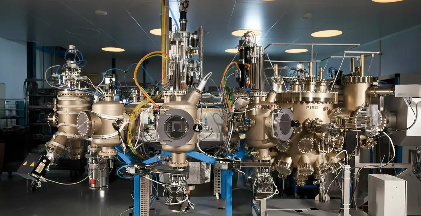
Molecular Beam Epitaxy (MBE) is a conventional technology for the epitaxial growth process developed in the 1960s. Using ultra-high vacuum (UHV), it produces high-purity crystalline thin films with atomic layer accuracy in terms of thickness, composition and doping concentration.
This precise control facilitates a fine matching of device electrical and optical properties, as well as, in the case of III–V semiconductor films, advanced bandgap engineering. These desirable attributes make MBE the preeminent method for growing high-quality epitaxial layers. Now that defines the performance of various devices such as LEDs, GaAs solar cells, photodetectors, sensors, lasers and power electronics.
But they have some significant disadvantages, high capital cost, complexity of operation and low growth rate, which induce impediment to industrial manufacture at a large scale. Require any help with MBE tool installation, calibration or fab floor setup? Our Global Field Engineering and Fab Facility Solutions teams are here to assist.
History and Evolution of Molecular Beam Epitaxy (MBE) Technology
The idea of Molecular Beam Epitaxy (MBE) was first proposed by K.G. Günther in 1958. Although not epitaxial (growth on glass), his films were built on by John Davey and Titus Pankey to show the now familiar MBE growth of epitaxial GaAs thin films deposited onto single crystal GaAs substrates in 1968.
The ultimate development of the technology was developed in the late 1960s by Arthur and Cho, who utilised Reflection High Energy Electron Diffraction (RHEED) as an in-situ growth monitoring technique for MBE. If your company is utilising legacy MBE platforms or you are considering an upgrade, our Legacy Tool Management Services will support ensuring continuity and the long life of the tool.
Why GaAs Is the Foundation of MBE-Grown III–V Semiconductor Devices
GaAs was the first compound semiconductor successfully grown by MBE and is still one of the most significant III–V compound semiconductors applied in high-performance optoelectronic devices, including solar cells, photodetectors, laser diodes and quantum devices.
GaAs has been employed for a wide range of applications thanks to its numerous beneficial characteristics, which include an energy gap of 1.43 eV with a direct transition nature, high electron mobility and absorption coefficient, as well as radiation tolerance, among others; these include devices such as space photovoltaics, infrared detectors and future quantum technologies.
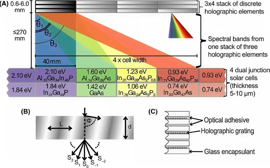
Being the first material to be studied in great detail with MBE, GaAs is thus extraordinarily well-characterised and has been the subject of several decades of research for epitaxial devices. Efficiencies of up to 15–20% were achieved in the 1980s for GaAs heterojunction solar cells grown on Ge substrates.
Challenges and Performance Trade-Offs in MBE-Grown GaAs Devices
While present efficiencies are among the highest in the industry, growing GaAs solar cells using MBE has advantages and drawbacks of its own.
- Throughput and cost: From a commercial point of view, MBE is less attractive for vapour-phase growth than other methods because of slow growth rates and high costs. Normal MBE growth rates are in the 1.0 μm/h range, which is much slower than those for CVD and MOCVD of 200 μm/h.
- Thickness and uniformity: Absorber layers for solar cells may be several microns thick. Achieving good thickness uniformity on wafers at this scale is difficult for MBE systems.
- Defect control: thin films consist of defects, such as dislocations, antisite defects, point defects and background impurities, etc. These defects decrease carrier lifetimes, resulting in decreases in open-circuit voltage and fill factor in optoelectronic devices. Consequently, the quality of the substrate, sharpness of interfaces and optimisation in growth conditions are important.
- Doping and alloying: We excel in doping and alloying of III–V compounds by MBE. Bandgap Engineering allows for broader absorption scenarios in solar. However, with the multi-junction and tandem cell structures to manage such issues as strain control, phase separation, and accurate compositional control become obstacles.
- Surface and interface quality: interfacial strain and recombination losses are major problems in stacks of multilayer solar cells. MBE’s rapid shutter control and ultra-high vacuum condition make the interfaces sharp, which can contribute to high-performance devices.
Many of the advantages of MBE are neutralised by its difficulties, causing it to be considered as more of a hybrid growth technique for commercial applications. This has led to the use of higher-throughput MOVPE/MOCVD techniques, often together with MBE for performance-critical layers.
Optoelectronic Devices Enabled by MBE-Grown III–V Heterostructures
Besides GaAs solar cells, MBE has shown remarkable utility for high-quality growth of device-grade III–V heterostructures in the context of various optoelectronic and electronic devices:
- LASERs and VCSELs: Laser-based on AlGaAs/GaAs heterostructures MBE have been extensively used for quantum well lasers and VCSELs. These devices show low threshold currents, continuous-wave operation up to high temperature and the modulation speed can be at the GHz level.
- Quantum Cascade LASERs (QCLs): mid-infrared QCLs can be made using GaAs/AlGaAs heterostructures grown by MBE. Fine control over the interface results in lower roughness and increased device performance.
- Infrared Photodetectors: The best IR detectors, such as HgCdTe (MCT) are MBE grown on GaAs substrates. InAs/GaSb superlattices grown on (0 1>)-oriented GaSb(001) substrates for GaSb-based nBn detectors and the effect of an engineered buffer layer to reduce lattice mismatch.
- High-mobility 2D electron gas (2DEG) heterostructures: Perhaps the most significant contribution of MBE has been in creating ultra-high-mobility 2D electron gas systems, which are indispensable for High Electron Mobility Transistors (HEMTs). The highest electron mobilities (~35 × 10⁶ cm²/V·s) have been achieved for MBE-grown AlGaAs/GaAs heterostructures.
The Role of Molecular Beam Epitaxy in Advanced GaAs and III–V Semiconductor Devices
Molecular Beam Epitaxy is a difficult and slow growth process which has typically been limited to the R&D laboratory environment. On the other hand, up to now, it would be unlikely that the crystallographic quality and purity of MBE-grown layers could be surpassed, providing crucial benefits towards new generations of semiconductor devices.
Industrial part implementation of MBE has been realized over the past decade, where state-of-the-art performance for device operation is preferred over throughput limitations. However, due to low wafer throughput, full-scale mass implementation is still unlikely; as such the MBE continues to be an enabling technology for device discovery and innovation.
With 15+ years of expertise and a global team of 500+ engineers, Orbit & Skyline is a trusted partner in the semiconductor industry. If you are looking for a semiconductor services and solution partner, reach out to us at hello@orbitskyline.com.

 Semiconductor FAB Solutions
 OEM Solutions