
Ensuring Vacuum Integrity in Semiconductor Manufacturing with Helium Leak Detectors
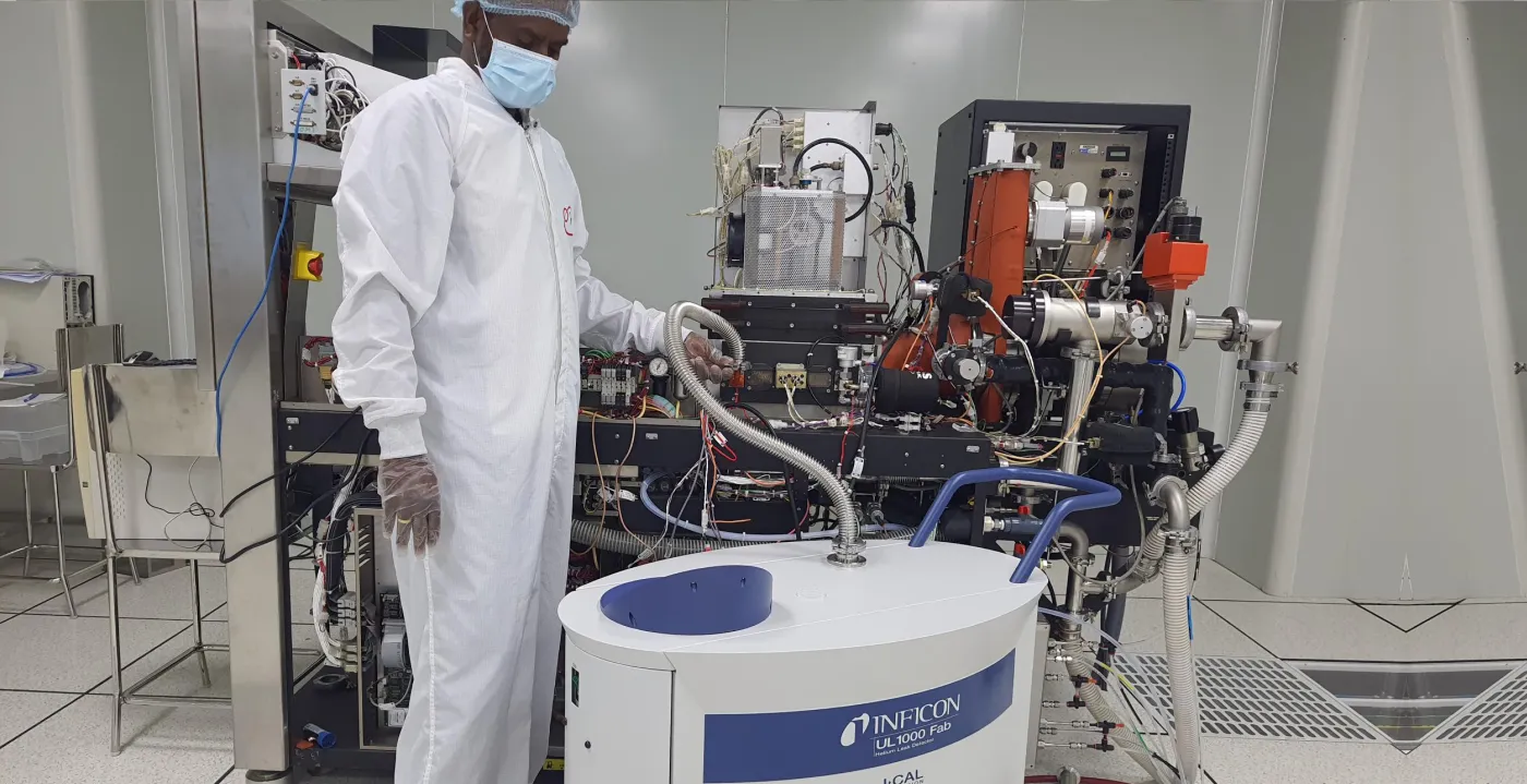
In the high-stakes world of semiconductor manufacturing, even the smallest gas leak can disrupt process integrity, reduce yield, and damage expensive equipment. One of the most critical tools in a semiconductor fab’s maintenance arsenal is the helium leak detector, a precision instrument used to verify vacuum integrity.
This blog will walk you through the basics of vacuum, types of helium leak detectors, real-world use cases, and how to perform a leak check on semiconductor tools to ensure optimal vacuum integrity and process reliability.
Understanding Vacuum Levels in Semiconductor Manufacturing
Semiconductor processes like etching, deposition, and ion implantation require precise environments where gas composition and pressure are tightly controlled. To achieve this, tools operate under different vacuum levels:
| Vacuum Type | Pressure Range (approx.) | Common Application |
|---|---|---|
| Rough Vacuum | 10³ to 1 mbar | Pump-down stage, load locks |
| Medium Vacuum | 1 to 10⁻³ mbar | Transfer chambers |
| High Vacuum | 10⁻³ to 10⁻⁷ mbar | Deposition/etch process chambers |
| Ultra-High Vacuum | <10⁻⁷ mbar | Ion implantation, electron beam |
| Types of Vacuum Used in Semiconductor Manufacturing | ||
Maintaining these vacuum levels is vital to prevent contamination and ensure process consistency. That’s where helium leak detectors come in.
What Is a Helium Leak Detector?
A helium leak detector is a mass spectrometer tuned to detect helium atoms. Helium is ideal because:
- It is inert and safe.
- It does not naturally occur in significant quantities in ambient air.
- It has a small atomic size, making it an excellent tracer gas.
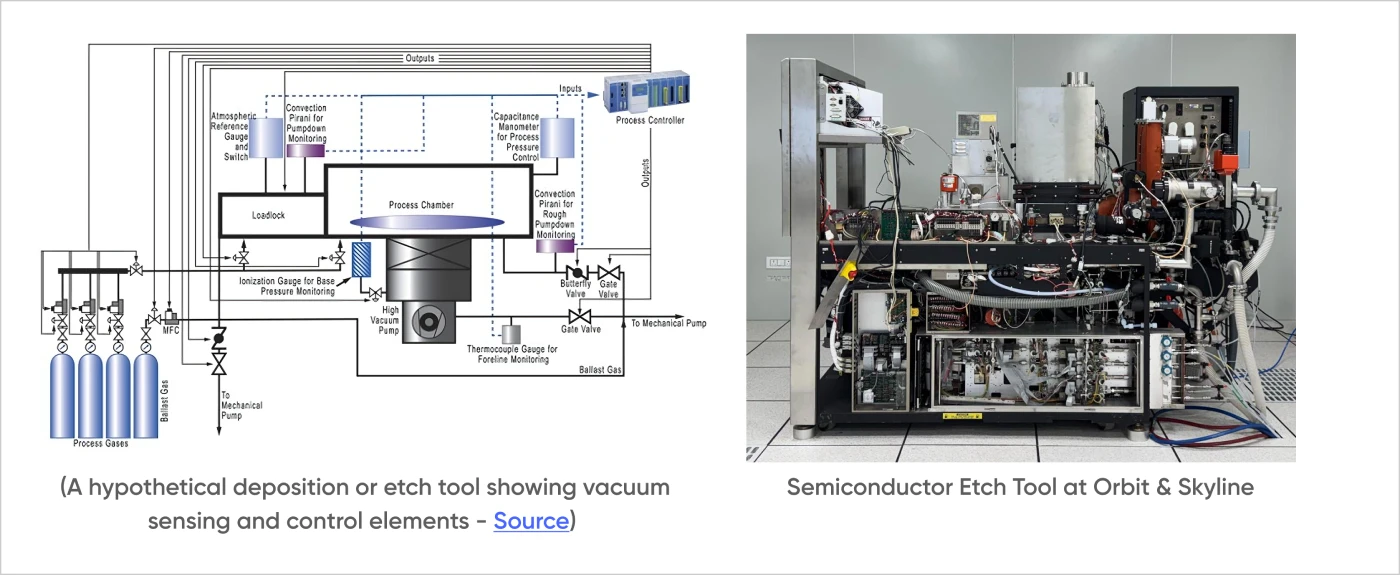
The detector identifies helium that escapes through leaks, indicating where vacuum integrity is compromised. It can detect leaks as small as 10-12 mbar·l/s, making it highly sensitive.
Types of Helium Leak Detection Methods
Leak detectors are broadly classified based on how helium is introduced and detected.
1. Vacuum Mode (Inside-Out Testing)
Helium is sprayed outside the chamber while the detector is connected to the vacuum side.
Models
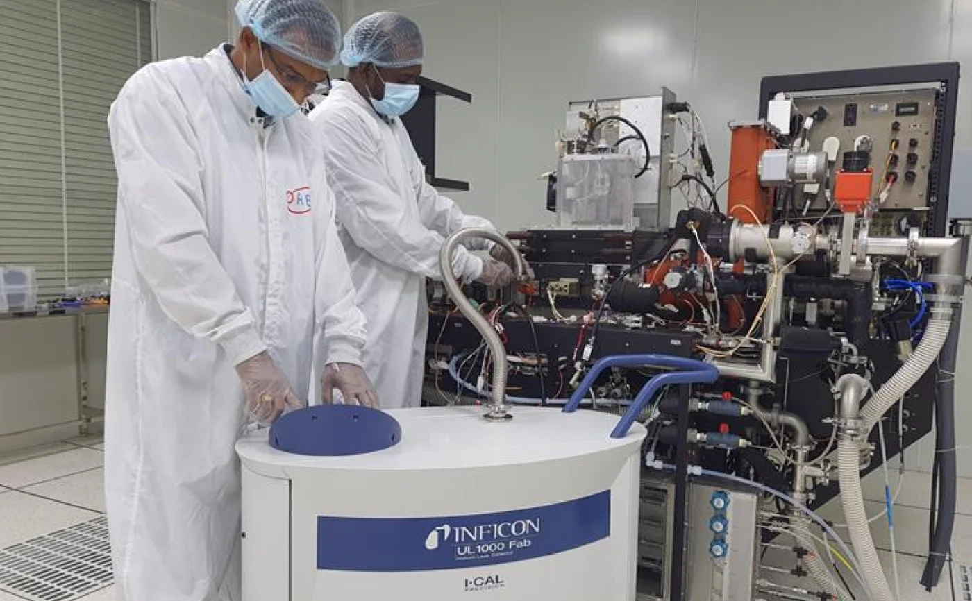
- INFICON UL1000 Fab: The INFICON UL1000 Fab is the standard for vacuum leak testing in semiconductor manufacturing, featuring dry compressing fore vacuum pumps, ultra-sensitive detection limits of <5·10-12 mbar·L/s, fast pump down, selectable background suppression (iZERO), and a manoeuvrable design, ideal for cleanroom maintenance and leak testing of vacuum tools.

- Pfeiffer ASM 340: Compact, portable leak detector ideal for industrial and cleanroom applications with fast response and high accuracy.

- Leybold Phoenix Quadro: The PHOENIX Quadro is part of Leybold’s latest generation of helium leak detectors, combining ultra-high helium sensitivity with fast response times, intuitive touchscreen controls, Wi-Fi login, and flexible data logging, ideal for semiconductor, R&D, and industrial applications.

2. Sniffer Mode (Outside-In Testing)
Helium is pressurised inside the component, and the detector “sniffs” for helium escaping to the outside.
Models
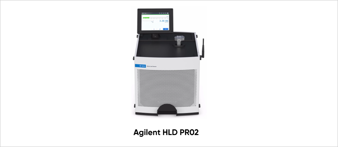
- Agilent HLD PR02: The Agilent HLD PR02 is a compact, portable helium mass spectrometer leak detector equipped with an intuitive 8.4-inch touchscreen, a built-in DS 40M rotary vane pump (2 m³/h), and advanced application setup guides—ideal for high-sensitivity leak detection with a sensitivity of 5×10⁻¹² mbar·L/s.
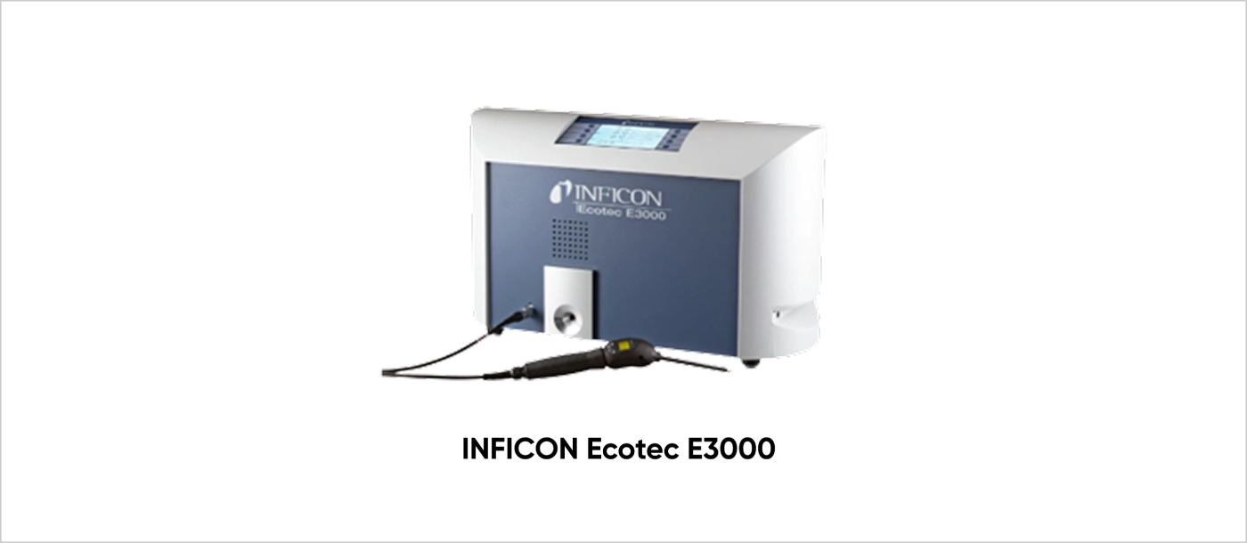
- INFICON Ecotec E3000: The INFICON Ecotec E3000 is a multi-gas sniffer leak detector tailored for high-throughput production lines. With IGS technology, ergonomic probe control, fast 0.8s response time, and helium sensitivity down to 1E-6 mbar·L/s, it ensures precise, efficient, and operator-friendly leak testing.
3. Integral Mode
Used for large systems, such as vacuum vessels. The entire volume is pressurised with helium, and the leak rate is measured cumulatively.
Applications of Helium Leak Detectors in Semiconductor Fabs:
- Etch/Deposition Chambers: Ensure process chambers maintain high or ultra-high vacuum levels.
- Load Locks & Transfer Chambers: Detect O-ring, gasket, and weld leaks that may cause contamination.
- Gas Panels & Welded Lines: Validate gas system integrity before introducing process gases.
- Cryo Pumps & Turbo Pumps: Periodic checks to maintain long-term vacuum system reliability.
- OEM Acceptance Testing: Final vacuum certification during tool manufacturing and before shipment.
How to Perform Helium Leak Testing on Semiconductor Tools
The following step-by-step procedure outlines how to perform a helium leak check using the vacuum mode:
- Pump Down: Bring the tool to its operational vacuum level.
- Connect the Leak Detector: Attach it to the chamber exhaust or test port.
- Stabilize Background Reading: Allow the detector to settle before testing.
- Spray Helium Around: Target areas such as flanges, welds, viewports, O-rings, and gas feedthroughs.
- Observe the Reading: If the leak rate spikes when helium is sprayed at a location, a leak is present.
- Quantify the Leak: Classify if it’s within the acceptable leak rate (typically <10⁻⁹ mbar·l/s).
- Document and Fix: Record the leak data, repair the issue, and retest the system.
Best Practices for Vacuum Leak Testing
- Avoid excessive helium spray to prevent false positives.
- Use a fine nozzle for pinpoint application.
- Log readings for traceability and compliance.
Key Takeaways
- Helium leak detection is essential for maintaining vacuum integrity in semiconductor fabs.
- Semiconductor vacuum systems require highly sensitive leak testing methods.
- Vacuum leak testing improves contamination control and process reliability.
- Helium leak detectors help maintain stable ultra-high vacuum environments.
- Regular semiconductor equipment maintenance reduces downtime and yield loss.
Conclusion
Helium leak detectors play a vital role in safeguarding the integrity of semiconductor manufacturing environments. By ensuring vacuum systems remain leak-free, they help maintain the ultra-clean conditions essential for high-yield and defect-free chip production. As semiconductor fabs grow more complex and precise, proactive leak detection isn’t just routine maintenance; it’s a cornerstone of quality, reliability, and operational excellence.
At Orbit & Skyline, our experts use advanced helium leak detection techniques to ensure optimal vacuum integrity across fab equipment, process chambers, and gas systems, supporting semiconductor leaders with precision-driven maintenance and engineering solutions.
With 15+ years of expertise and a global team of 600+ engineers, Orbit & Skyline is a trusted partner in the semiconductor industry. If you are looking for a semiconductor services and solution partner, reach out to us at hello@orbitskyline.com.

 Semiconductor FAB Solutions
 OEM Solutions